Moore's Law: The Driving Force Behind Computing Evolution
What Is Moore's Law?
Moore's Law is the observation that the number of transistors on an integrated circuit doubles approximately every two years. This trend has fueled exponential growth in computing power while keeping costs relatively stable.
First articulated by Gordon Moore, co-founder of Intel, this principle has shaped the semiconductor industry for over five decades. It is not a physical law but rather an economic and engineering trend that has driven innovation in technology.
The Origin and Evolution of Moore's Law
Gordon Moore's Prediction
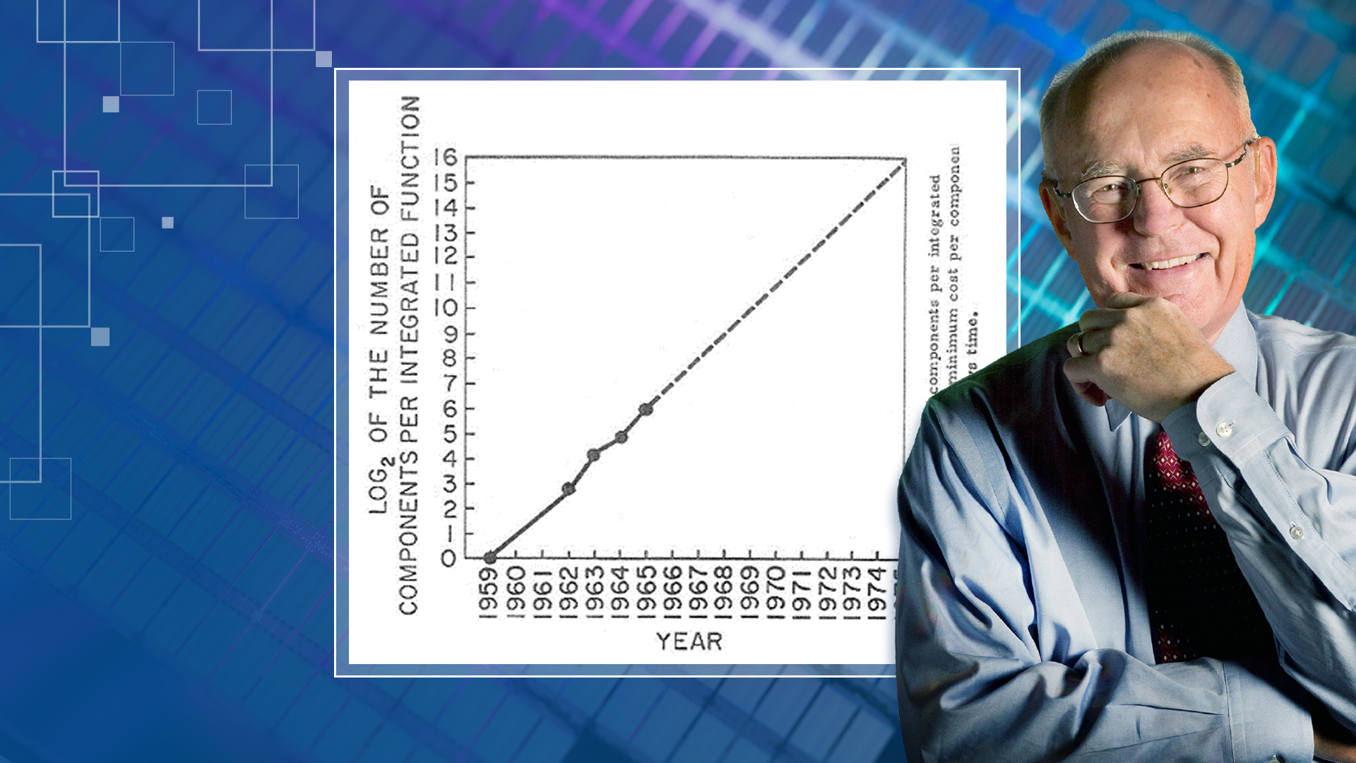
In 1964, Gordon Moore, then R&D director at Fairchild Semiconductor, presented his observations in a talk. He later formalized them in a 1965 article titled "Cramming More Components onto Integrated Circuits."
Initially, Moore predicted that the number of transistors would double every year for the next decade. However, in 1975, he revised this timeline to every two years, a prediction that held true for much longer than anticipated.
From Theory to Industry Standard
What began as an observation quickly became a self-fulfilling prophecy for the semiconductor industry. Companies like Intel adopted Moore's prediction as a development goal, ensuring that computing power grew exponentially.
This trend replaced bulky, room-sized computers and vacuum tubes with compact, affordable chips, revolutionizing the electronics industry.
Key Milestones in Moore's Law
Transistor Growth Over the Decades
The progression of transistor counts has been staggering:
- 1960s: Early chips contained only a handful of transistors.
- 2010s: Chips reached billions of transistors.
- 2024: A single chip achieved 4 trillion transistors.
Impact on Computing Power
As transistor counts increased, so did computational capacity. From 1975 to 2009, computing power doubled approximately every 1.5 years.
This exponential growth enabled the development of personal devices, mobile technology, and the infrastructure of the Information Age.
How Moore's Law Shaped Modern Technology
From Mainframes to Smartphones
Moore's Law made it possible to shrink computers from room-sized mainframes to handheld smartphones. This miniaturization was driven by the ability to pack more transistors into smaller spaces.
The shift from vacuum tubes to integrated circuits marked a turning point in computing history, making technology more accessible and affordable.
Software and Parallel Processing
As hardware advanced, software evolved to leverage multi-core processors. This shift toward parallel processing allowed applications to run faster and more efficiently.
Today, even everyday devices like smartphones and laptops benefit from the computational power enabled by Moore's Law.
Challenges to Moore's Law
Physical and Economic Limits
Despite its longevity, Moore's Law faces growing challenges. As transistors approach sub-2nm scales, quantum effects and physical limitations make further miniaturization difficult.
Additionally, the breakdown of Dennard scaling means that energy efficiency no longer improves proportionally with transistor size reductions.
Memory and Performance Gaps
Another hurdle is the memory bandwidth gap, where CPU performance grows exponentially while memory improvements remain linear. This disparity creates bottlenecks in system performance.
Innovations like 3D stacking and advanced manufacturing nodes are helping to sustain progress, but the future of Moore's Law remains a topic of debate.
"Moore's Law only stops when innovation stops."
This statement underscores the ongoing efforts to push the boundaries of semiconductor technology, ensuring that Moore's Law continues to drive progress in computing.
Conclusion
Moore's Law has been a cornerstone of technological advancement, shaping the modern world in ways that were once unimaginable. While challenges exist, the spirit of innovation continues to propel the semiconductor industry forward.
In the next section, we will explore the current trends and future possibilities that could extend or redefine Moore's Law for the next generation of computing.
The Future of Moore's Law: Innovations and Alternatives
Beyond Traditional Scaling
As traditional transistor scaling approaches its limits, the semiconductor industry is exploring new avenues to sustain Moore's Law. One promising direction is 3D chip stacking, which allows for more transistors in a given space by building vertically rather than horizontally.
Another approach is the development of chiplets, modular components that can be combined to create more powerful and efficient processors. This method reduces manufacturing complexity while maintaining performance gains.
Specialized Architectures and AI Accelerators
The rise of artificial intelligence has led to the creation of AI accelerators, specialized hardware designed to handle machine learning tasks more efficiently than traditional CPUs. These chips optimize performance for specific workloads, reducing reliance on raw transistor counts.
Companies like NVIDIA and Google have invested heavily in these architectures, demonstrating that innovation can continue even as Moore's Law faces physical constraints.
Quantum Computing: A Potential Leap Forward
Understanding Quantum Bits (Qubits)
Quantum computing represents a radical departure from classical computing. Instead of bits, which are either 0 or 1, quantum computers use qubits, which can exist in a superposition of states. This allows for probabilistic problem-solving at speeds unattainable by traditional systems.
While still in its infancy, quantum computing could eventually overcome some of the limitations of Moore's Law by solving complex problems in fields like cryptography, material science, and optimization.
Challenges in Quantum Computing
Despite its potential, quantum computing faces significant hurdles. Qubit stability remains a major issue, as quantum states are highly susceptible to environmental interference. Additionally, scaling quantum systems to practical sizes requires breakthroughs in error correction and cooling technologies.
Researchers are actively working on these challenges, with companies like IBM and Google leading the charge in developing viable quantum processors.
Performance-per-Watt: The New Metric for Progress
Shifting Focus from Raw Power to Efficiency
As transistor density reaches its limits, the industry is increasingly prioritizing performance-per-watt over sheer computational power. This shift reflects the growing demand for energy-efficient devices, particularly in mobile and IoT applications.
Improving efficiency not only extends battery life but also reduces heat generation, a critical factor in maintaining system stability and longevity.
Heterogeneous Computing
Heterogeneous computing combines different types of processors, such as CPUs, GPUs, and AI accelerators, to optimize performance for diverse workloads. This approach maximizes efficiency by assigning tasks to the most suitable hardware.
For example, a smartphone might use a GPU for graphics-intensive tasks while relying on a low-power CPU for everyday operations. This flexibility is key to sustaining progress in the post-Moore's Law era.
Industry Perspectives on Moore's Law
Is Moore's Law Dead?
The question of whether Moore's Law is dead has sparked intense debate. Some argue that the slowdown in transistor scaling marks the end of the era, while others believe that innovation will find new ways to sustain the trend.
Intel, a company deeply tied to Moore's Law, has acknowledged the challenges but remains committed to pushing the boundaries of semiconductor technology. Their roadmap includes advanced packaging techniques and new materials to extend the law's relevance.
Expert Opinions and Predictions
Experts offer varied perspectives on the future of Moore's Law:
- Optimists point to emerging technologies like quantum computing and neuromorphic chips as potential successors.
- Pragmatists argue that while transistor scaling may slow, system-level innovations will continue to drive progress.
- Skeptics suggest that the economic and physical constraints may eventually render Moore's Law obsolete.
"The death of Moore's Law has been predicted many times, but each time, the industry has found a way to adapt and innovate."
This sentiment highlights the resilience of the semiconductor industry and its ability to evolve in the face of challenges.
The Role of Moore's Law in the Digital Age
Enabling the Internet of Things (IoT)
Moore's Law has been instrumental in the rise of the Internet of Things (IoT), where billions of connected devices rely on compact, powerful, and energy-efficient chips. From smart home devices to industrial sensors, IoT applications benefit from the continuous improvements in semiconductor technology.
As IoT expands, the demand for smaller, more efficient processors will only grow, further emphasizing the need for innovations that sustain Moore's Law.
Cloud Computing and Data Centers
The exponential growth in computing power has also fueled the expansion of cloud computing. Data centers, which power everything from social media to enterprise applications, depend on high-performance processors to handle massive workloads.
Even as Moore's Law faces challenges, advancements in chip design and manufacturing will continue to support the scalability and efficiency of cloud infrastructure.
Conclusion: The Legacy and Future of Moore's Law
Moore's Law has been a driving force behind the technological revolution of the past half-century. While its future may be uncertain, the principles it represents—innovation, efficiency, and progress—remain as relevant as ever.
In the final section, we will explore the broader implications of Moore's Law and its lasting impact on society, economy, and technology.
The Societal and Economic Impact of Moore's Law
Transforming Industries and Daily Life
Moore's Law has reshaped nearly every aspect of modern life. From healthcare to finance, industries have leveraged exponential computing power to innovate and streamline operations. Medical imaging, genetic sequencing, and drug discovery have all benefited from faster, more efficient processors.
In everyday life, smartphones, laptops, and smart devices have become indispensable, all made possible by the relentless progress predicted by Moore's Law. The digital revolution has democratized access to information, entertainment, and communication.
Economic Growth and Job Creation
The semiconductor industry, driven by Moore's Law, has become a cornerstone of the global economy. It has created millions of jobs in manufacturing, research, and software development. Countries like the United States, South Korea, and Taiwan have built thriving tech economies around chip production.
Startups and established companies alike have capitalized on the increasing computational power to develop new products and services. The rise of Silicon Valley as a global tech hub is closely tied to the advancements enabled by Moore's Law.
Environmental Considerations and Sustainability
The Energy Challenge
While Moore's Law has driven incredible technological progress, it has also contributed to growing energy consumption. Data centers, which power cloud computing and digital services, now account for a significant portion of global electricity use. The push for performance-per-watt is not just about efficiency but also about sustainability.
Companies are increasingly focusing on green computing initiatives, such as using renewable energy sources and improving cooling technologies to reduce the carbon footprint of data centers.
E-Waste and Recycling
The rapid pace of technological advancement has led to a surge in electronic waste (e-waste). As devices become obsolete more quickly, the challenge of recycling and disposing of old electronics has grown. Governments and organizations are working to implement better e-waste management practices.
Innovations in modular design and repairability are also emerging as ways to extend the lifespan of electronic devices, reducing the environmental impact of the tech industry.
Moore's Law in Education and Research
Advancing Scientific Discovery
The exponential growth in computing power has accelerated scientific research across disciplines. Fields like astronomy, climate modeling, and particle physics rely on high-performance computing to process vast amounts of data and simulate complex systems.
For example, the Large Hadron Collider generates petabytes of data that require advanced processors to analyze. Similarly, climate scientists use supercomputers to model weather patterns and predict long-term environmental changes.
Revolutionizing Education
Moore's Law has also transformed education by making powerful computing tools accessible to students and researchers. Online learning platforms, virtual labs, and educational software have democratized knowledge, allowing people worldwide to access high-quality education.
Institutions are leveraging AI and machine learning to personalize learning experiences, adapting to individual student needs and improving educational outcomes.
The Global Race for Semiconductor Dominance
Geopolitical Implications
The semiconductor industry has become a critical arena for global competition. Countries recognize that dominance in chip manufacturing translates to economic and military advantages. The United States, China, and the European Union are investing heavily in domestic semiconductor production.
Supply chain disruptions, such as those experienced during the COVID-19 pandemic, have highlighted the strategic importance of semiconductor self-sufficiency. Governments are offering incentives to attract chip manufacturers and reduce reliance on foreign suppliers.
Innovation and Collaboration
Despite geopolitical tensions, collaboration remains essential for advancing semiconductor technology. International partnerships in research and development have led to breakthroughs in materials science, manufacturing techniques, and chip design.
Industry consortia and academic collaborations continue to drive innovation, ensuring that the principles of Moore's Law endure even as the challenges mount.
Looking Beyond Moore's Law: The Next Frontier
Neuromorphic Computing
Inspired by the human brain, neuromorphic computing aims to create processors that mimic biological neural networks. These chips could revolutionize AI by enabling more efficient and adaptive learning systems.
Companies like IBM and Intel are already developing neuromorphic chips, which promise to deliver significant performance improvements for tasks like pattern recognition and real-time data processing.
Photonics and Optical Computing
Another promising avenue is optical computing, which uses light instead of electricity to perform calculations. Photonics-based processors could overcome the speed limitations of traditional silicon chips, enabling faster and more energy-efficient computing.
Research in this field is still in its early stages, but the potential for breakthroughs is immense, particularly in areas like high-speed communications and quantum computing.
Conclusion: The Enduring Legacy of Moore's Law
Moore's Law has been one of the most influential principles in the history of technology. For over five decades, it has guided the semiconductor industry, driving unprecedented advancements in computing power, efficiency, and affordability.
While the physical and economic challenges to sustaining Moore's Law are real, the spirit of innovation it represents continues to thrive. The industry's shift toward performance-per-watt, heterogeneous computing, and emerging technologies like quantum computing and neuromorphic chips ensures that progress will continue.
Key Takeaways
- Moore's Law has shaped the modern world by enabling exponential growth in computing power.
- Challenges like quantum effects and energy efficiency are pushing the industry toward new innovations.
- Emerging technologies, including quantum computing and neuromorphic chips, could redefine the future of computing.
- The societal and economic impact of Moore's Law is profound, influencing industries, education, and global competition.
- Sustainability and environmental considerations are becoming increasingly important in the evolution of semiconductor technology.
"Moore's Law may slow, but the march of progress will not stop. The next era of computing will be defined by creativity, collaboration, and a relentless pursuit of innovation."
As we look to the future, the legacy of Moore's Law serves as a reminder of what is possible when vision, ambition, and ingenuity come together. The journey of technological advancement is far from over, and the best may still be yet to come.


Walter Brattain: A Pioneer in the Field of Semiconductors
In the annals of scientific history, certain names stand out not only for their intellectual brilliance but also for their profound impact on the technological landscape of the modern world. Walter Houser Brattain is one such name. A co-inventor of the point-contact transistor, Brattain's work fundamentally shaped the world of electronics, enabling the proliferation of devices that define our daily lives today. While his scientific achievements are well-documented, the man behind the experiments, his journey, and his contributions beyond the laboratory are equally compelling narratives.
Early Life and Education
Born on February 10, 1902, in Amoy, China, Walter Brattain was the son of American missionaries Ross R. Brattain and Ottilie Houser Brattain. The Brattain family returned to the United States when Walter was a small child, settling in Washington State. The environment of the Pacific Northwest, with its burgeoning educational opportunities and natural beauty, provided a fertile ground for Brattain’s intellectual curiosity to flourish.
Brattain pursued his higher education at Whitman College, where he earned his Bachelor of Science in 1924. His academic journey did not stop there; he went on to receive a Master of Arts from the University of Oregon in 1926, followed by a Ph.D. in physics from the University of Minnesota in 1929. It was during these formative years at these institutions that Brattain honed the skills and deepened the scientific curiosity that would later drive his groundbreaking experiments.
Professional Career and Achievements
Following his doctoral studies, Walter Brattain embarked on a professional journey that would lead him to one of the most significant scientific breakthroughs of the 20th century. His early career was marked by a series of positions that allowed him to delve into diverse areas of physics research. However, it was his tenure at Bell Telephone Laboratories, beginning in 1929, that proved to be the defining period of his career.
At Bell Labs, Brattain was part of a dynamic team that included notable physicists such as John Bardeen and William Shockley. It was within this intellectually stimulating environment that Brattain, along with his collaborators, embarked on the quest to solve one of the pressing challenges of the time: finding a reliable and efficient replacement for vacuum tubes in electronic devices.
The Invention of the Transistor
The invention of the point-contact transistor in 1947 marked a watershed moment in the history of electronics and telecommunications. This tiny device, underpinned by semiconductor materials, would revolutionize the way that electronic signals were amplified and switched. Together with Bardeen and Shockley, Brattain spearheaded the development of this remarkable innovation.
The point-contact transistor they created was a small, yet powerful, device that allowed for the manipulation of electrical signals in a way that was faster and more reliable than the bulky and less efficient vacuum tubes of the time. The profound implications of this invention were not immediately apparent to the general public, but it laid the foundational stone for the eventual miniaturization and sophistication of modern electronic devices, including computers and mobile phones.
Recognition and Legacy
In 1956, Walter Brattain, along with his colleagues John Bardeen and William Shockley, was awarded the Nobel Prize in Physics for their seminal work on semiconductor technology and the invention of the transistor. This prestigious recognition cemented their status as luminaries of modern science and highlighted the immense potential of solid-state physics.
Brattain's contributions extended beyond his scientific achievements; he was a respected educator and mentor who believed in the dissemination of knowledge. After retiring from Bell Labs in 1967, Brattain joined Whitman College as an adjunct professor, where he continued to inspire and nurture the curiosity of future scientists.
Walter Brattain's journey from a curious young boy in China to a Nobel Laureate in Physics is a testament to his unwavering dedication to scientific exploration and innovation. His groundbreaking work on the transistor not only transformed the field of electronics but also laid the groundwork for the technological advancements that define our contemporary world. As we continue to build upon his legacy, Walter Brattain remains an enduring symbol of the power of human ingenuity and collaboration.
The Transistor: Impact and Evolution
The transistor, initially a product of experimental physics, quickly transitioned to being a pivotal component in the technology sector. The device's ability to function as an amplifier or a switch made it indispensable in myriad applications, from telecommunications to data processing systems. In the decades following its invention, the point-contact transistor underwent significant evolution, spurring an era of technological innovation.
The immediate impact of the transistor was felt in the telecommunications industry, where it replaced vacuum tubes in telephone exchanges, making systems more reliable and efficient. However, the true transformative power of the transistor was realized in the realm of computing. The miniaturization of transistors enabled the development of integrated circuits (ICs), which are foundational to modern computers. This leap in technology paved the way for the birth of the computer age and, subsequently, the digital era.
As transistors shrank in size and increased in efficiency, they became integral to the development of smaller, more powerful computing devices. This miniaturization accelerated exponentially, a phenomenon famously chronicled by "Moore's Law," which predicted the doubling of transistors on integrated circuits roughly every two years. The exponential growth in transistor density has led to the creation of microprocessors that are orders of magnitude more powerful than the early computing machines.
Brattain’s Influence on Semiconductor Research
Beyond his direct involvement in the invention of the transistor, Walter Brattain's influence extended into the wider realm of semiconductor research. His work emphasized the importance of understanding the fundamental properties of materials, which has been an enduring theme in the field of solid-state physics. Brattain's experiments underscored the significance of choosing appropriate semiconductor materials and understanding their surface states, which directly influenced the behavior of transistors.
His pioneering research laid the groundwork for subsequent discoveries and innovations in semiconductors. Understanding how electrons moved within semiconductor materials allowed scientists to engineer electronic devices with enhanced capabilities. This essential knowledge contributed to developments in fields as diverse as electronics, renewable energy, and quantum computing.
Brattain’s commitment to experimental rigor and his collaborative spirit also set a precedent in scientific research. His partnership with other notable scientists, such as John Bardeen, showcased the power of collaborative inquiry and cross-disciplinary insights in achieving breakthroughs. This model of collaborative research is now a cornerstone of modern scientific inquiry, catalyzing advancements across various fields.
A Legacy of Innovation and Education
Walter Brattain’s scientific legacy is interwoven with his dedication to education and science communication. After retiring from Bell Labs, he devoted much of his time to academia, teaching and mentoring the next generation of scientists at Whitman College. His approach to teaching was deeply rooted in the belief that exposing students to experimental methodologies and encouraging curiosity were paramount to scientific advancement.
Brattain’s commitment to education was not limited to formal classroom settings. He often engaged with educators and academics to promote science literacy among the public. He believed that the accessibility of scientific knowledge was crucial for fostering a society capable of informed decision-making in an increasingly technological world.
Beyond his scientific pursuits, Brattain was known for his humility and willingness to acknowledge the contributions of others. This was evident in his speeches and writings, where he often credited his colleagues and the collective efforts of many for the success of the transistor project. His ability to combine intellectual curiosity with generosity of spirit made him a respected figure among peers and a valued mentor.
Personal Life and Interests
Outside the laboratory, Walter Brattain led a life characterized by various personal interests and a deep connection to family. His upbringing in the Pacific Northwest instilled in him a love for nature, which endured throughout his life. Brattain was an avid outdoorsman, often spending time hiking, fishing, and enjoying the natural beauty surrounding his Washington home.
He was also a man of varied interests, with a keen appreciation for music and literature. This breadth of interests allowed him to connect with a wide array of individuals, endearing him to colleagues and friends alike.
Walter Brattain married twice; his first marriage was to Katherine Blood, with whom he had a son, William G. Brattain. After Katherine's passing, Brattain later married Emma Jane (Bettie) Walkinshaw. His family life provided him with stability and joy, which he often credited as essential supports throughout his demanding career.
In summation, Walter Brattain’s contributions to the field of semiconductors and his role in developing the transistor were transformative. His work enabled countless innovations that shape the technological vistas of today, from computing to mobile communications. However, his legacy extends beyond his scientific contributions, encompassing his dedication to education, commitment to collaboration, and personal virtues that inspired those who knew him. As technology continues to evolve, Brattain's pioneering spirit remains an enduring beacon of innovation and intellectual exploration.
Societal Impact and the Transistor Revolution
The ripple effects of Walter Brattain's work on the transistor extend far beyond the realms of physics and electronics engineering. The transistor, a small yet monumental invention, catalyzed a global transformation, ushering in the digital revolution that has reshaped our societal structures and economies. Its influence pervades every aspect of modern life, propelling advancements in communication, healthcare, education, and beyond.
Transistors enabled the development of compact, reliable electronic devices, leading to the proliferation of consumer electronics such as radios, televisions, and eventually, personal computers. These devices have fundamentally changed how people interact, consume information, and entertain themselves, embedding technology into the fabric of daily life. As mobile devices became ubiquitous, powered by ever-smaller and more powerful transistors, the way humans communicate and connect has been transformed, transcending geographical and cultural barriers.
The healthcare industry has also greatly benefited from transistor technology, with medical equipment becoming more sophisticated and accessible. Imaging technologies like MRIs and CT scans rely heavily on the precision and power of modern electronics, allowing for earlier diagnostics and more effective treatments. Moreover, wearable health devices and telemedicine platforms are revolutionizing patient care, enabling continuous monitoring and remote consultations that reduce barriers to healthcare access.
Transistors and the Future of Technology
As society continues to evolve, the foundational contributions of Walter Brattain and his colleagues remain deeply relevant. Transistors are at the heart of current developments in cutting-edge technologies like artificial intelligence (AI), the Internet of Things (IoT), and quantum computing. These fields leverage the microelectronic advancements driven by transistors to push the boundaries of what is technologically possible.
AI, with its ability to process vast amounts of data and learn from patterns, relies heavily on powerful computing capabilities. Transistors, through integrated circuits and microprocessors, provide the computational backbone needed to drive AI technologies. The scalability and efficiency of AI applications in fields such as autonomous vehicles, personalized medicine, and smart cities are direct beneficiaries of Brattain's work on transistors.
In the realm of IoT, devices embedded with sensors and connected through vast networks improve efficiency and resource utilization in sectors like agriculture, transportation, and infrastructure. The minute scale and low power requirements of transistors make these widespread networks feasible, contributing to the creation of interconnected systems that enhance productivity and sustainability.
Quantum computing, a field still in its nascent stages, promises to revolutionize computing by leveraging quantum states to perform complex computations at unprecedented speeds. While fundamentally different from classical transistors, developments in semiconductor materials and understanding gleaned from traditional transistor research underpin many quantum computing advances, indicating a lineage traceable to Brattain's early work.
The Human Element
Amidst the staggering technological developments initiated by the transistor, the human element of Walter Brattain's story remains paramount. His journey exemplifies the quintessential scientific pursuit—navigating complex challenges with perseverance, curiosity, and collaboration. The narrative of the transistor is as much about human ingenuity and tenacity as it is about technical prowess.
Brattain, remembered for his modesty and collaborative nature, often emphasized the importance of teamwork and shared knowledge in achieving great scientific feats. His interactions with colleagues at Bell Labs and later, his role as an educator, showcased a scientist deeply committed to the ethos of continuous learning and knowledge sharing. This approach not only bolstered his scientific contributions but also inspired a culture of openness and cooperation in research communities worldwide.
Enduring Lessons and Inspirations
Walter Brattain’s life and achievements offer enduring lessons and inspirations for aspiring scientists and technologists. His humble beginnings, academic dedication, and eventual rise to a Nobel Laureate reflect the potential within individuals to achieve greatness regardless of origins. His work underscores the importance of collaboration and the cross-pollination of ideas, essential elements in addressing today’s complex, interdisciplinary challenges.
Moreover, Brattain's commitment to education highlights the necessity of investing in the development of future generations, fostering inquisitiveness and scientific literacy that empower individuals to solve pressing global issues. His legacy serves as a reminder of the profound impact that one individual’s contributions can have on society, echoing across time and technology.
In conclusion, Walter Brattain’s contributions to science and society extend far beyond the invention of the transistor. His work has empowered generations of innovation, creating tools and technologies that are vital to modern life. As technology continues to advance at a rapid pace, Brattain's pioneering spirit remains a guiding light, inspiring innovation, collaboration, and a relentless pursuit of knowledge.


RAPTOR AI: La Revolución en Detección de Defectos en Semiconductores
Introducción a RAPTOR AI
La industria de los semiconductores enfrenta desafíos crecientes en la detección de defectos y la autenticación de componentes. RAPTOR AI emerge como una solución innovadora que combina imágenes ópticas y modelos de aprendizaje profundo para identificar alteraciones físicas y falsificaciones con una precisión del 97.6% en pruebas de laboratorio.
Desarrollada por investigadores de la Universidad de Purdue, esta tecnología utiliza nanopartículas de oro como huellas físicas únicas, lo que permite una detección no destructiva y altamente precisa.
¿Qué es RAPTOR AI?
Definición y Origen
RAPTOR significa residual attention-based processing of tampered optical responses. Es una metodología basada en deep learning que utiliza un mecanismo de atención residual para comparar respuestas ópticas antes y después de la manipulación.
Esta tecnología fue desarrollada por el grupo de Alexander Kildishev en la Universidad de Purdue y publicada en la revista Advanced Photonics. Actualmente, hay una patente pendiente para esta innovación.
Método Físico
RAPTOR AI emplea nanopartículas de oro integradas en los chips semiconductores como huellas físicas únicas. Estas partículas se capturan mediante microscopía de campo oscuro para registrar su distribución.
Cualquier alteración en esta distribución indica manipulación o falsificación, lo que permite una detección precisa y confiable.
Rendimiento y Precisión
Resultados de Laboratorio
En pruebas de laboratorio, RAPTOR AI ha demostrado una precisión de detección del 97.6% en escenarios de peor caso. Esta precisión supera a métodos tradicionales como Hausdorff, Procrustes y Average Hausdorff en márgenes que van del 6% al 40%.
Estos resultados destacan la efectividad de RAPTOR AI en comparación con técnicas geométricas tradicionales.
Latencia y Throughput
La cadena de procesamiento de RAPTOR AI incluye segmentación semántica, construcción de matrices de distancias y un clasificador convolucional residual. En pruebas de laboratorio, la latencia por muestra ha sido inferior a 100 ms en hardware de consumo, con una verificación total cercana a 80 ms.
Estos tiempos de procesamiento son compatibles con las tasas de producción industrial, lo que facilita su integración en flujos de control de calidad automatizados.
Contexto Industrial
Problemas en la Industria de Semiconductores
La industria global de semiconductores, valorada en cientos de miles de millones de dólares, enfrenta riesgos significativos debido a defectos de fabricación y la proliferación de chips falsificados. Estos problemas afectan la fiabilidad y seguridad en sectores críticos como la aeronáutica, infraestructura y defensa.
Las técnicas actuales de inspección tienen limitaciones para distinguir entre degradación natural y manipulación deliberada, y muchas soluciones no escalan bien en entornos industriales.
Ventajas de RAPTOR AI
RAPTOR AI se posiciona como un complemento o alternativa a métodos geométricos y de inspección por rayos X. Su principal ventaja es la no destructividad, ya que utiliza microscopía de campo oscuro en lugar de técnicas ionizantes.
Además, ofrece una alta especificidad frente a la manipulación y tiene un gran potencial para la integración en flujos de control de calidad automatizados.
Implementación Práctica
Incorporación de Nanopartículas
Para utilizar RAPTOR AI, es necesario incorporar nanopartículas de oro en el proceso de fabricación o empaquetado de los chips. Estas partículas actúan como huellas físicas únicas que permiten la autenticación y detección de manipulaciones.
Este proceso requiere cambios en la cadena de suministro y en los procedimientos de prueba para aprovechar plenamente la técnica.
Flujo de Captura de Imagen
El método de RAPTOR AI requiere un flujo de captura de imagen de referencia para cada unidad. Esto implica la creación y almacenamiento seguro de bases de datos de referencia que puedan ser utilizadas para la verificación y autenticación de los componentes.
La implementación práctica de RAPTOR AI, por lo tanto, involucra no solo cambios técnicos, sino también logísticos y de gestión de datos.
Tendencias Actuales
Convergencia de IA y Metrología Óptica
RAPTOR AI encaja en la tendencia creciente de combinar inteligencia artificial con técnicas de imagen óptica y tomografía X para la inspección no destructiva y la detección temprana de fallos en semiconductores y empaquetado avanzado.
Esta convergencia permite una mayor precisión y eficiencia en la detección de defectos, lo que es crucial para la industria de semiconductores.
Enfoque en Seguridad de la Cadena de Suministro
Tras problemas recientes con componentes falsos y riesgos geopolíticos, la demanda de técnicas de autenticación física a prueba de clonación ha aumentado. RAPTOR AI se presenta como una respuesta directa a esta demanda, ofreciendo una solución robusta y escalable.
La tecnología de huellas físicas con nanopartículas y la inspección automatizada son clave para garantizar la seguridad y autenticidad de los componentes semiconductores.
Desafíos y Limitaciones de RAPTOR AI
Validación en Entornos Industriales
Aunque los resultados de laboratorio son prometedores, con una precisión del 97.6%, la implementación en líneas de producción reales presenta desafíos significativos. Los entornos industriales introducen variables como ruido, variaciones en los procesos de fabricación y posibles ataques adversariales que podrían afectar el rendimiento de RAPTOR AI.
Es crucial realizar pruebas a gran escala y validaciones independientes para asegurar que la tecnología mantenga su eficacia en condiciones del mundo real.
Cambios en los Procesos de Fabricación
La incorporación de nanopartículas de oro en los chips semiconductores requiere modificaciones en los flujos de fabricación y empaquetado. Esto implica no solo cambios técnicos, sino también logísticos y de gestión de la cadena de suministro.
Los fabricantes deberán adaptar sus procesos para incluir la inserción de nanopartículas y establecer protocolos para la creación y almacenamiento seguro de las huellas de referencia.
Robustez Frente a Adversarios Sofisticados
Aunque RAPTOR AI ha demostrado resiliencia frente a ciertos tipos de manipulación, como abrasión y calentamiento, su capacidad para resistir intentos deliberados y evolucionados de falsificación aún necesita ser evaluada continuamente.
Los falsificadores podrían desarrollar técnicas más avanzadas para eludir la detección, lo que requerirá actualizaciones y mejoras constantes en los modelos de aprendizaje profundo de RAPTOR AI.
Comparación con Otras Tecnologías de Detección
Métodos Geométricos Tradicionales
Los métodos geométricos, como las distancias de Hausdorff y Procrustes, han sido ampliamente utilizados en la detección de defectos en semiconductores. Sin embargo, RAPTOR AI supera estas técnicas en márgenes significativos, con mejoras reportadas del 6% al 40% en las métricas de precisión.
La principal ventaja de RAPTOR AI es su capacidad para detectar manipulaciones sutiles que podrían pasar desapercibidas para los métodos geométricos tradicionales.
Inspección por Rayos X
La inspección por rayos X es otra técnica común en la industria de semiconductores. Aunque efectiva, esta método es destructivo y requiere equipos costosos y especializados.
RAPTOR AI, en cambio, utiliza microscopía de campo oscuro, una técnica no destructiva que puede integrarse más fácilmente en los flujos de producción existentes sin dañar los componentes.
Técnicas de Autenticación Física
Las técnicas de autenticación física, como las funciones físicas no clonables (PUFs), han ganado popularidad en los últimos años. RAPTOR AI se basa en un enfoque similar, utilizando nanopartículas de oro como huellas físicas únicas.
Esta tecnología ofrece una capa adicional de seguridad al combinar la autenticación física con modelos de aprendizaje profundo, lo que mejora la precisión y la confiabilidad de la detección.
Impacto en la Seguridad de la Cadena de Suministro
Reducción de Chips Falsificados
La proliferación de chips falsificados representa una amenaza significativa para la industria de semiconductores. Estos componentes pueden comprometer la seguridad y la fiabilidad de sistemas críticos en sectores como la aeronáutica, la defensa y la infraestructura.
RAPTOR AI ofrece una solución robusta para combatir este problema, permitiendo la detección precisa de componentes falsificados y mejorando la integridad de la cadena de suministro.
Mejora en la Confiabilidad de los Componentes
La confiabilidad de los componentes semiconductores es esencial para el funcionamiento seguro y eficiente de dispositivos electrónicos. Los defectos de fabricación y las manipulaciones deliberadas pueden afectar negativamente esta confiabilidad.
Con RAPTOR AI, los fabricantes pueden identificar y eliminar componentes defectuosos o falsificados antes de que lleguen al mercado, lo que mejora la calidad y la confiabilidad de los productos finales.
Cumplimiento de Normativas y Estándares
La industria de semiconductores está sujeta a normativas y estándares estrictos que buscan garantizar la seguridad y la calidad de los componentes. La implementación de RAPTOR AI puede ayudar a los fabricantes a cumplir con estas regulaciones al proporcionar una herramienta efectiva para la detección de defectos y la autenticación de componentes.
Además, la tecnología puede ser adaptada para satisfacer los requisitos específicos de diferentes normativas, lo que facilita su adopción en diversos mercados y sectores.
Futuro de RAPTOR AI en la Industria
Potencial de Escalabilidad
Uno de los principales desafíos para la adopción de RAPTOR AI es su escalabilidad. Aunque las pruebas de laboratorio han demostrado tiempos de procesamiento compatibles con las tasas de producción, la implementación a gran escala requerirá inversiones significativas en infraestructura y capacitación.
Sin embargo, el potencial de escalabilidad de RAPTOR AI es prometedor, especialmente si se logra integrar la tecnología en los flujos de producción existentes sin disruptar significativamente los procesos actuales.
Integración con Otras Tecnologías
RAPTOR AI no está destinado a reemplazar completamente las técnicas existentes de detección de defectos, sino a complementarlas. La integración con otras tecnologías, como la inspección por rayos X y los métodos geométricos, puede proporcionar una solución más completa y robusta para la detección de defectos y la autenticación de componentes.
Esta integración podría mejorar aún más la precisión y la eficiencia de los procesos de control de calidad en la industria de semiconductores.
Desarrollos Futuros y Mejoras
El campo de la inteligencia artificial y el aprendizaje profundo está en constante evolución. Los desarrollos futuros en estos campos podrían llevar a mejoras significativas en la precisión y la eficiencia de RAPTOR AI.
Además, la investigación continua en la resistencia a ataques adversariales y la adaptación a nuevas técnicas de falsificación será crucial para mantener la relevancia y la efectividad de RAPTOR AI en el futuro.
Casos de Uso y Aplicaciones
Aeronáutica y Defensa
En sectores críticos como la aeronáutica y la defensa, la confiabilidad y la seguridad de los componentes semiconductores son de suma importancia. La implementación de RAPTOR AI puede ayudar a garantizar que los componentes utilizados en estos sectores sean auténticos y libres de defectos.
Esto no solo mejora la seguridad de los sistemas, sino que también reduce el riesgo de fallos catastróficos que podrían tener consecuencias graves.
Electrónica de Consumo
En la electrónica de consumo, la calidad y la autenticidad de los componentes son esenciales para la satisfacción del cliente y la reputación de la marca. RAPTOR AI puede ser utilizado para detectar y eliminar componentes falsificados o defectuosos antes de que lleguen a los productos finales.
Esto no solo mejora la calidad de los productos, sino que también reduce los costos asociados con devoluciones y reparaciones.
Infraestructura Crítica
La infraestructura crítica, como los sistemas de energía y comunicaciones, depende en gran medida de la confiabilidad de los componentes semiconductores. La implementación de RAPTOR AI puede ayudar a garantizar que estos sistemas funcionen de manera segura y eficiente.
La detección temprana de defectos y manipulaciones puede prevenir fallos que podrían tener un impacto significativo en la sociedad y la economía.
Conclusiones Preliminares
Beneficios Clave de RAPTOR AI
- Alta precisión de detección del 97.6% en pruebas de laboratorio.
- Técnica no destructiva que utiliza microscopía de campo oscuro.
- Capacidad para detectar manipulaciones sutiles que podrían pasar desapercibidas para métodos tradicionales.
- Potencial para integrarse en flujos de producción existentes sin disruptar significativamente los procesos actuales.
Desafíos a Superar
- Validación en entornos industriales con variables del mundo real.
- Cambios en los procesos de fabricación y gestión de la cadena de suministro.
- Resistencia a ataques adversariales y técnicas de falsificación evolucionadas.
- Inversiones significativas en infraestructura y capacitación para la implementación a gran escala.
Perspectivas Futuras
RAPTOR AI representa un avance significativo en la detección de defectos y la autenticación de componentes semiconductores. Su capacidad para combinar imágenes ópticas con modelos de aprendizaje profundo ofrece una solución robusta y escalable para los desafíos actuales de la industria.
Con el desarrollo continuo y la integración con otras tecnologías, RAPTOR AI tiene el potencial de convertirse en un estándar en la industria de semiconductores, mejorando la seguridad, la confiabilidad y la calidad de los componentes electrónicos.
Implicaciones Económicas y de Mercado
Impacto en la Industria de Semiconductores
La industria global de semiconductores, valorada en cientos de miles de millones de dólares, se beneficia directamente de tecnologías como RAPTOR AI. La reducción de chips falsificados y defectuosos puede generar ahorros significativos al disminuir los costos asociados con devoluciones, garantías y fallos en el campo.
Además, la mejora en la confiabilidad de los componentes puede aumentar la competitividad de los fabricantes, permitiéndoles ofrecer productos de mayor calidad y seguridad.
Reducción de Costos Operativos
La implementación de RAPTOR AI puede llevar a una reducción de costos operativos en varias áreas. La detección temprana de defectos y manipulaciones permite a los fabricantes evitar costos de reprocesamiento y desperdicio de materiales.
Además, la automatización de los procesos de inspección puede reducir la necesidad de intervención manual, lo que se traduce en una mayor eficiencia y menores costos laborales.
Nuevas Oportunidades de Mercado
La adopción de RAPTOR AI puede abrir nuevas oportunidades de mercado para los fabricantes de semiconductores. La capacidad de ofrecer componentes con autenticación y detección de defectos avanzada puede ser un diferenciador clave en sectores críticos como la aeronáutica, la defensa y la infraestructura.
Además, la tecnología puede ser licenciada o vendida como un servicio, generando nuevas fuentes de ingresos para las empresas que la desarrollan y implementan.
Consideraciones Éticas y de Seguridad
Protección de la Propiedad Intelectual
La implementación de RAPTOR AI plantea preguntas importantes sobre la protección de la propiedad intelectual. Las huellas físicas únicas creadas por las nanopartículas de oro pueden ser utilizadas para autenticar componentes, pero también requieren medidas robustas para proteger la integridad de estas huellas.
Es crucial establecer protocolos seguros para el almacenamiento y manejo de las bases de datos de referencia, evitando que sean comprometidas o utilizadas de manera fraudulenta.
Privacidad y Manejo de Datos
La recolección y almacenamiento de datos de referencia para la autenticación de componentes plantea preocupaciones sobre la privacidad y el manejo de datos. Los fabricantes deben asegurar que los datos sean manejados de manera segura y conforme a las regulaciones de protección de datos.
La implementación de medidas de cifrado y control de acceso es esencial para garantizar que la información no sea accesible a partes no autorizadas.
Responsabilidad y Cumplimiento Normativo
La adopción de RAPTOR AI también implica consideraciones sobre la responsabilidad y el cumplimiento normativo. Los fabricantes deben asegurar que la tecnología cumpla con los estándares y regulaciones aplicables en los mercados donde operan.
Además, es importante establecer claras políticas de responsabilidad en caso de fallos o falsificaciones que no sean detectadas por la tecnología.
Estudios de Caso y Ejemplos Prácticos
Implementación en la Industria Aeronáutica
Un ejemplo práctico de la implementación de RAPTOR AI es su uso en la industria aeronáutica. Los componentes semiconductores utilizados en aviones y sistemas de navegación deben ser de la más alta calidad y confiabilidad.
La tecnología puede ser utilizada para autenticar y detectar defectos en estos componentes, asegurando que cumplan con los estándares de seguridad y rendimiento requeridos.
Aplicación en Dispositivos Médicos
En el sector de dispositivos médicos, la confiabilidad de los componentes semiconductores es crítica. La implementación de RAPTOR AI puede ayudar a garantizar que los dispositivos médicos, como marcapasos y equipos de diagnóstico, funcionen de manera segura y efectiva.
La detección de defectos y manipulaciones en estos componentes puede prevenir fallos que podrían tener consecuencias graves para la salud de los pacientes.
Uso en Infraestructura de Telecomunicaciones
La infraestructura de telecomunicaciones depende en gran medida de la confiabilidad de los componentes semiconductores. La implementación de RAPTOR AI puede ayudar a garantizar que los sistemas de telecomunicaciones funcionen de manera continua y sin interrupciones.
La detección temprana de defectos y manipulaciones puede prevenir fallos que podrían afectar la conectividad y la comunicación en grandes áreas geográficas.
Conclusión: El Futuro de RAPTOR AI
Resumen de Beneficios Clave
RAPTOR AI representa un avance significativo en la detección de defectos y la autenticación de componentes semiconductores. Entre sus beneficios clave se incluyen:
- Una precisión de detección del 97.6% en pruebas de laboratorio.
- Una técnica no destructiva que utiliza microscopía de campo oscuro.
- La capacidad de detectar manipulaciones sutiles que podrían pasar desapercibidas para métodos tradicionales.
- El potencial para integrarse en flujos de producción existentes sin disruptar significativamente los procesos actuales.
Desafíos y Oportunidades
Aunque RAPTOR AI ofrece numerosas ventajas, también enfrenta desafíos significativos. La validación en entornos industriales, los cambios en los procesos de fabricación y la resistencia a ataques adversariales son áreas que requieren atención continua.
Sin embargo, las oportunidades que ofrece esta tecnología son inmensas. Desde la mejora en la seguridad y confiabilidad de los componentes hasta la reducción de costos operativos y la apertura de nuevas oportunidades de mercado, RAPTOR AI tiene el potencial de transformar la industria de semiconductores.
Recomendaciones para la Industria
Para aprovechar al máximo el potencial de RAPTOR AI, los fabricantes de semiconductores deben considerar las siguientes recomendaciones:
- Invertir en pruebas y validaciones a gran escala para asegurar la eficacia de la tecnología en entornos industriales.
- Adaptar los procesos de fabricación para incluir la inserción de nanopartículas de oro y la creación de bases de datos de referencia.
- Establecer protocolos seguros para el manejo y almacenamiento de datos de autenticación.
- Colaborar con desarrolladores de tecnología y reguladores para asegurar el cumplimiento normativo y la protección de la propiedad intelectual.
Palabras Finales
En un mundo donde la confiabilidad y la seguridad de los componentes semiconductores son más importantes que nunca, RAPTOR AI emerge como una solución innovadora y prometedora. Su capacidad para combinar imágenes ópticas con modelos de aprendizaje profundo ofrece una herramienta poderosa para la detección de defectos y la autenticación de componentes.
Con el desarrollo continuo y la adopción generalizada, RAPTOR AI tiene el potencial de convertirse en un estándar en la industria de semiconductores, mejorando la calidad, la seguridad y la confiabilidad de los productos electrónicos en todo el mundo. La tecnología no solo beneficia a los fabricantes, sino también a los consumidores finales, asegurando que los dispositivos que utilizan sean seguros y confiables.
